SDIO Protocol is a widely used Bus for the interfacing modem (device) to the application processor (Host). SDIO Protocol is used for Data exchange between host and device. Initially, the SDIO Protocol bus used operates at 50MHz (SD2.0) Specification. The current generation system uses a 200MHz (UHS I) SD3.0 bus.
Like SD, SDIO Protocol capable host generates the Clock Signal at 400 kHz and scales up to the specific frequency as per the standard supported by the device. The Host issues specific commands over the CMD line and decides the next course of action based on the Response received by the Device. SDIO uses either 1-bit or 4-bit data transfer between the host and the device.
SDIO Introduction:
SDIO offers extended capability to what the SD Card offers by providing High-Speed Data I/O Functions separately or combined with memory capability within the Card. Host devices supporting SDIO can connect the SD Slot with I/O devices like Bluetooth, Wireless LAN, GPS Receiver, Digital Camera, etc. As many as seven Functions can be mapped into the SDIO I/O.
SDIO Interface Bus:
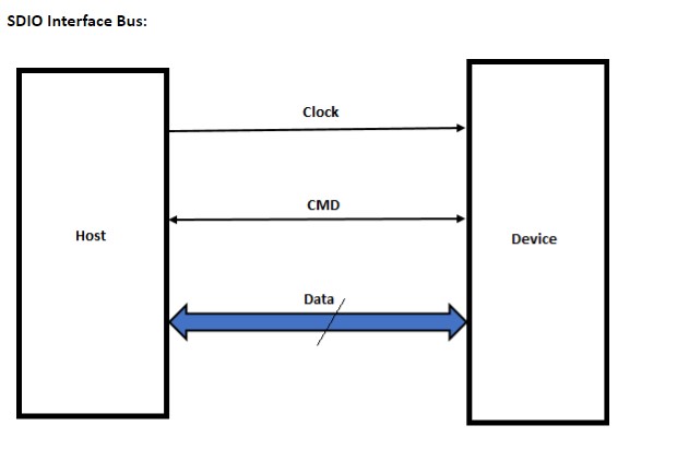
SDIO Bus has a clock, command, and 4-bit data bus-wide. SDIO provides the flexibility to switch at different speeds ranging 25MHz to 200MHz, bus mode in SDR /DDR, and bus width at 1-bit or 4-bit. This offers an application to use the bus-appropriate mode without consuming many system resources and power.
SDIO card types and data rates:
SDIO supports multiple card types with different Data Rates and Signaling Modes.
The below table provides a detailed comparison of different SDIO Interfaces along with Maximum Data Rates supported and Signaling Levels.
| SDIO Card Type | Mode | Interface | Clock Range | Maximum Data Rate | Signaling Mode |
| Non UHS | Low Speed | SPI | 0-400 KHz | 200 KB/s | 3.3 V |
| 1-Bit SD | |||||
| Optional 4-Bit SD | |||||
| Non UHS | Full Speed | SPI | 0 -25 MHz | 12.5 MB/s | |
| 1-Bit SD | |||||
| 4-Bit SD | |||||
| Non UHS | High Speed | 4-Bit SD | 0 – 50 MHz | 25 MB/s | |
| UHS-I | Full Speed | SPI | 0 -25 MHz | 12.5 MB/s | 3.3V |
| 1-Bit SD | |||||
| 4-Bit SD | |||||
| High Speed | 4-Bit SD | 0 – 25 MHz | 25 MB/s | 3.3V | |
| SDR12 | 4-Bit SD | 0 -208 MHz | 12.5 MB/s | 1.8V | |
| SDR25 | 4-Bit SD | 25 MB/s | |||
| SDR50 | 4-Bit SD | 50 MB/s | |||
| DDR50 | 4-Bit SD | 50 MB/s | |||
| SDR104 | 4-Bit SD | 104 MB/s | |||
| UHS-II * | FD156 | 4-Bit SD | 0-52 MHz | 156 MB/s | 0.4V LVDS |
| HD312 | 4-Bit SD | 312 MB/s |
- UHS-II is backward compatible with UHS-I.
- Prodigy supports up to UHS-I Protocol Analysis with PGY-SSM and UHS-II Protocol Analysis with PGY UHS-II Protocol Analyzer.
SDIO Command Set: Theory of Operations
SDIO introduces IO_SEND_OP_COND (CMD5) to inquire about the Voltage Range needed by the I/O Card. SDIO also adds two more data transfer Command instructions to support the I/O functionality. These Commands are IO_RW_DIRECT (CMD52) is a Fast I/O access command and IO_RW_EXTENDED (CMD53) allows Fast access with Byte or Block addresses.
CMD5: IO_SEND_OP_COND
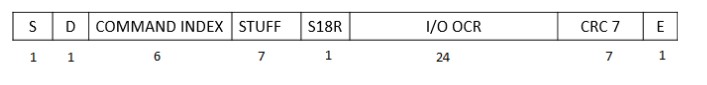
- CMD5 is identified by 6-bit Command Index set at 000101b.
- The supported minimum and maximum values of VDD are set in the I/O OCR Register which is a 24-bit Register in CMD5.
- S18R is the Switching to 1.8V request bit
R4: Response to IO_SEND_OP_COND
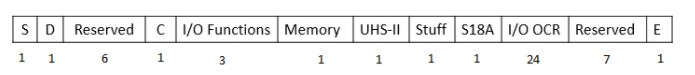
- I/O Functions is a 3-bit field and indicates the number of I/O Functions supported by the Card.
- S18A is set indicating switching to 1.8V is accepted by the device.
- I/O OCR indicates the supported Range of Voltages supported.
CMD52: IO_RW_DIRECT
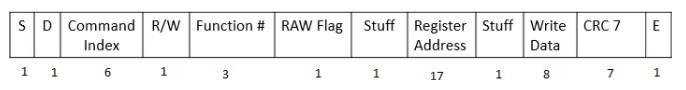
The following operations are accomplished by CMD52 in SDIO by writing into specific bits in Common Command Code Register in Common I/O Area (CIA), which otherwise uses separate Commands in SD.
- I/O Reset
- Abort Block Transfer
- Set Block Length in Function Basic Register (FBR)
- Set Bus Width.
CMD53: IO_RW_EXTENDED
CMD53 provides the option to Read and Write multiple I/O Registers with a Single Command.
The Read and Write Single/Multiple Blocks is accomplished with the CMD53 command, unlike SD Card which uses multiple commands to accomplish this.
Challenges in SDIO Protocol Debug
IP development cycle would include IP RTL design and verification, Prototyping, tape out, electrical and Protocol Validation, driver software validation, and reliable system operation. At different stages, design and test/verification engineers face different types of bugs in the product. These are caused due to design, manufacturing processes, Operating Systems, and interoperability problems. A Firmware validation team would require the Protocol Analyzer to verify the effectiveness of the SDIO Controller Driver for a specific Operating System. To locate and identify these design bugs, a testing tool such as Protocol Analyzer plays a significant role. In the case of SDIO, based on electrical characteristics and Protocol, it offered significant challenges to debugging SDIO Protocol.
SD, SDIO Protocol Analyzer addresses the challenges effectively with Unlimited Protocol Capture Memory and a simple and easy-to-use GUI that provides a Listing Window of the decoded Protocol along with important features to locate specific User Events, Custom views, Advanced Triggers, Pin-Point Errors, Statistical analysis and Pictorial Protocol information with Histograms and Trend plots. This coupled with Offline Trace analysis capability makes PGY-SSM a versatile solution for multiple teams in different locations.
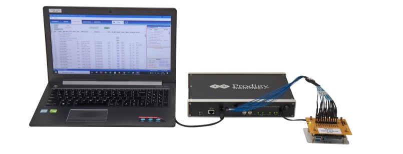
PGY-SSM Probe setup with DUT
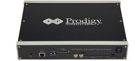
Image of Emmc Protocol Analyzer